
Precision Machining Solutions for Microelectronic Communication & Optical Equipment – Arui Precision
With the rapid advancement of 5G communications, micro‑semiconductors, and intelligent optical devices, equipment is increasingly trending toward miniaturization, integration, and ultra‑high reliability. This evolution places extremely stringent demands on dimensional accuracy, surface finish, and structural consistency of core components. Precision machining has become the critical manufacturing process for microelectronic communication hardware and optical equipment precision parts, directly determining signal transmission stability, imaging fidelity, and long‑term service life.
Unlike ordinary mechanical parts, microelectronic and optical hardware components are often micro‑thin‑walled structures, irregular micro‑cavities, and intricate snap‑fit features. Even the slightest dimensional deviation, burr, or flatness error can cause communication signal attenuation, optical imaging shift, assembly jamming, or even component failure. That is why such parts must rely on professional precision machining techniques and rigorous quality control systems to meet the mass‑production standards and application requirements of high‑end optoelectronic equipment.
Four Major Technical Challenges in Microelectronic & Optical Parts Machining
1. Thin‑Walled Structures Are Prone to Deformation – Precision Control Is Extremely Difficult
Products such as 5G communication bases, optical lens holders, and semiconductor micro‑mountings typically have ultra‑thin walls, slender geometries, and low rigidity. Conventional cutting forces easily cause elastic deformation or warping. Even minor machining errors can result in hole misalignment or excessive assembly clearance, directly affecting communication signal quality and optical focusing accuracy. Therefore, fixture design, toolpath optimization, and cutting stress management are key aspects of precision machining.
2. Micro‑Holes and Irregular Geometries – Very Little Tolerance for Error
Optical focusing assemblies, communication connector hardware, and micro‑signal shielding parts contain numerous micro‑holes, narrow slots, complex curved surfaces, and precision threads. Conventional 3‑axis machines with multiple setups accumulate positioning errors, making it impossible to guarantee hole coaxiality or slot parallelism. Only advanced precision machining methods such as 5‑axis simultaneous machining can complete all features in a single setup, eliminating cumulative errors.
3. Extremely Strict Surface Finish – No Burrs, No Contaminants
Optical precision parts must ensure no refraction or scattering in imaging, while communication hardware must maintain stable electrical conductivity and heat dissipation. Post‑machining surfaces must be free of tool marks, scratches, or burrs, with roughness strictly controlled. Moreover, the entire process must avoid metal dust and particle contamination, meeting clean‑room production standards.
4. High Batch‑to‑Batch Consistency – Dimensional Drift Must Be Prevented
Microelectronic communication equipment is typically mass‑produced, demanding extreme consistency across batches. Long‑run machine thermal deformation and slight tool wear can cause dimensional drift. This requires a mature process compensation system and high‑frequency calibration to guarantee zero‑defect output in every batch. Precision machining plays a pivotal role in maintaining such stability.
Arui Precision’s High‑Precision Machining Solutions
With 18 years of deep expertise in precision machining, Arui Precision specializes in high‑accuracy manufacturing of microelectronic communication hardware and optical equipment precision parts. Leveraging imported high‑end machines and a mature process system, we provide systematic solutions to the challenges above, consistently delivering micron‑grade quality.
Equipment: 5‑Axis, One‑Setup, Zero Positioning Error
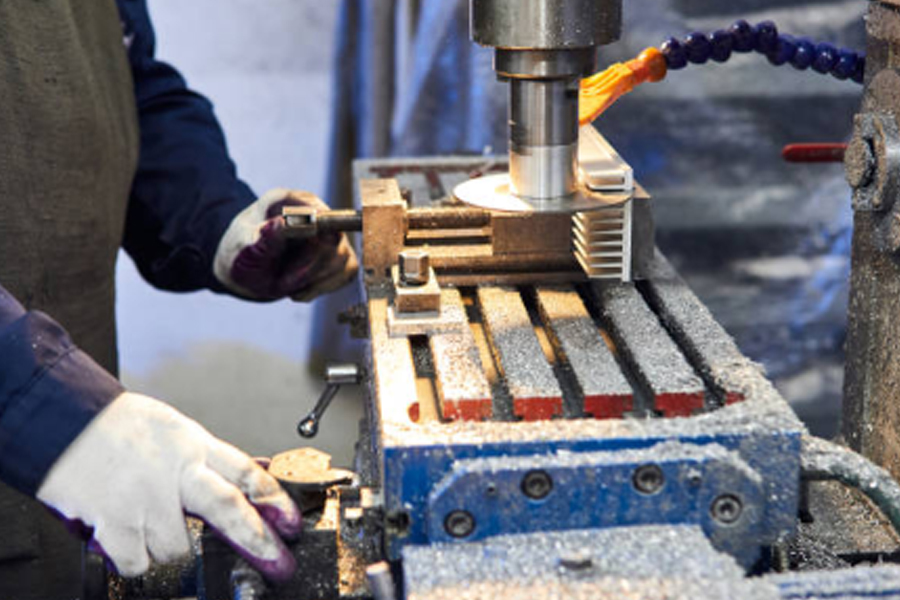
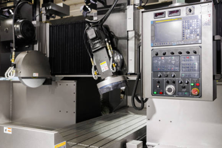
Our facility is equipped with over 300 units of advanced machinery, including German DMG Mori and American Haas 5‑axis machining centers, high‑speed engraving machines, Zeiss CMM coordinate measuring machines, and spectral inspection equipment. All precision machining tasks are performed in a single setup to machine multiple faces, micro‑holes, and complex surfaces simultaneously, completely eliminating positioning errors from multiple clampings. This hardware foundation guarantees that machining accuracy is stably maintained within ±0.02 mm.
Process Innovation: Stress‑Controlled, No Deformation in Thin Walls
For thin‑walled, easily deformable parts, we adopt layered micro‑cutting and high‑speed low‑load milling strategies, combined with custom flexible fixtures to distribute clamping stress. After machining, we apply constant‑temperature stress‑relief treatment to eliminate internal cutting stresses, preventing post‑processing distortion. We also continuously optimize micro‑tool parameters, monitor tool wear in real time, and apply backlash compensation – all essential elements of our precision machining excellence.
Quality Assurance: Full Traceability, Data‑Driven Inspection
We have established a comprehensive quality management system covering DQE, SQE, PQE, and CQE. Every batch of optical and microelectronic precision parts undergoes full CMM dimensional inspection, surface finish inspection, and cleanliness/contamination testing. All data are traceable, strictly aligning with high‑end optoelectronic industry standards.
Core Machining Categories – Covering Microelectronic & Optical Fields
Leveraging our mature precision machining capabilities, we can undertake custom manufacturing of various high‑end precision hardware for multiple industries:
- Microelectronic Communication: 5G communication base micro‑structures, signal‑shielding hardware, communication connector housings, precision terminal mounting brackets, microelectronic heat‑dissipation components, RF device precision fittings.
- Optical Equipment: Optical lens holders, focus‑adjustment bases, photoelectric sensor housings, precision optical retaining rings, inspection instrument light‑transmission parts, micro‑scope hardware components.
We support over 50 materials including stainless steel, aluminum alloys, copper, and engineering plastics, and offer 10+ high‑end surface finishing processes. Whether you need non‑standard customization, rapid prototyping, small‑to‑medium batches, or large‑scale mass production, we deliver efficiently.
Why Choose Arui Precision?
- Ultra‑high precision, stable output: Consistently achieves ±0.02 mm tolerance with excellent surface finish, no burrs, and no deformation – fully meeting the demanding requirements of optical imaging and signal transmission.
- One‑stop custom service: Integrated DFM optimization, precision machining, surface treatment, dimensional inspection, assembly, and packaging – significantly shortening R&D and production cycles.
- Full certifications & mass‑production capability: ISO9001 and ISO14001 certified; over 20,000 m² of standardized workshop space; delivering 150+ projects monthly – suitable for high‑end optoelectronic orders from domestic and overseas clients.
- Cost‑effective with export‑grade quality: Lean production reduces costs by 30% compared to European/American manufacturers, while maintaining internationally comparable quality. Products are exported to 30+ countries and regions.
Conclusion
The competitiveness of microelectronic communication and optical equipment ultimately depends on the machining precision and stability of their core components. With 18 years of high‑end manufacturing experience, Arui Precision focuses on precision machining of microelectronic communication hardware and optical equipment precision parts.
We have successfully overcome the challenges of thin‑walled micro‑structures, irregular micro‑holes, and ultra‑fine surface finishing, providing stable, efficient, and high‑precision custom component solutions for optoelectronic communication, microelectronics, and intelligent inspection equipment manufacturers. Choose Arui – choose reliability and excellence.